
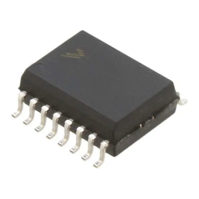
Imagens apenas para referência
MC68HC908QY2CDW
+Lista de MateriaisIC MCU 8BIT 1.5KB FLASH 16SOIC
-
FabricanteNXP USA Inc.
-
Peça do Fabricante #MC68HC908QY2CDW
-
Ficha Técnica MC68HC908QY2CDW DataSheet
-
Em Estoque8880
365 Garantia de Qualidade em 1 dia
7*24 Garantia de serviço em 24 horas
90-Garantia de pós-venda em 1 dia
Garantia de Produto Genuíno
Especificações
| Atributo | Valor |
| Series | HC08 |
| Part Status | Obsolete |
| Digi Key Programmable | Not Verified |
| Core Processor | HC08 |
| Core Size | 8-Bit |
| Speed | 8MHz |
| Peripherals | LVD, POR, PWM |
| Number of I/O | 13 |
| Program Memory Size | 1.5KB (1.5K x 8) |
| Program Memory Type | FLASH |
| RAM Size | 128 x 8 |
| Voltage - Supply (Vcc/Vdd) | 2.7V ~ 5.5V |
| Data Converters | A/D 4x8b |
| Oscillator Type | Internal |
| Operating Temperature | -40°C ~ 85°C (TA) |
| Mounting Type | Surface Mount |
| Supplier Device Package | 16-SOIC |
| Package / Case | 16-SOIC (0.295", 7.50mm Width) |
| Base Product Number | MC68HC908 |
Visão Geral
Description
Key features include a built-in 10-bit ADC, pulse-width modulation (PWM) outputs, and multiple I/O ports, which enable versatile interfacing options for sensors and actuators. The MC68HC908QY2CDW operates at a maximum clock speed of 8 MHz, ensuring adequate performance for various applications in automotive, industrial control, and consumer electronics.
Additionally, it supports a variety of communication protocols, enhancing its ability to interact with other devices in a system. The chip is well-suited for applications requiring low power consumption and operational efficiency, making it a popular choice for developers in embedded systems design.
Equivalent
Features
1. 8-bit Architecture: It utilizes an 8-bit CPU core for efficient processing.
2. Memory: It has 2 KB of Flash memory for program storage and 128 bytes of RAM for data.
3. I/O Ports: Offers multiple general-purpose I/O pins for interfacing with peripherals.
4. Timers: Equipped with a 16-bit timer for timing applications and event counting.
5. ADC: Features a 10-bit Analog-to-Digital Converter, allowing for analog signal processing.
6. Communication Interfaces: Supports serial communications such as UART.
7. Low Power Consumption: Designed for energy efficiency, suitable for battery-operated devices.
8. Operating Voltage: Typically operates at 2.7V to 5.5V.
9. On-chip Oscillator: Simplifies clock generation with an integrated oscillator.
These features make the MC68HC908QY2CDW suitable for various applications, including automotive, consumer electronics, and industrial control systems.
Pinout
Pin Count and Functions:
- Total Pins: 28
- Key Pin Functions:
- Digital I/O: Multiple pins serve as general-purpose Input/Output (GPIO).
- Analog-to-Digital Converter (ADC): Dedicated pins for analog input.
- Timer Functions: Pins for pulse-width modulation (PWM) and timer outputs.
- Serial Communication: Pins for UART (Universal Asynchronous Receiver-Transmitter) capabilities.
- Reset and Power: Includes pins for power supply and reset functionality.
- Clock Input: A pin for connecting an external clock source.
The MC68HC908QY2CDW is widely used in embedded applications due to its rich feature set and low power consumption.
Manufacturer
The MC68HC908QY2CDW is part of the HC08 family of microcontrollers, known for its 8-bit architecture and is commonly used in embedded systems. NXP's products are widely utilized in various industries, including automotive electronics, mobile communication, and consumer electronics, reflecting the company's commitment to innovation and technology advancement in semiconductor solutions.





