
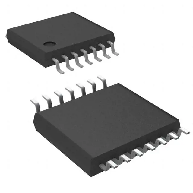
Imagens apenas para referência
NLSV4T244DTR2G
+Lista de MateriaisIC XLTR VL UNIDIR 14-TSSOP
-
Fabricanteonsemi
-
Peça do Fabricante #NLSV4T244DTR2G
-
Ficha Técnica NLSV4T244DTR2G DataSheet
-
Em Estoque9919
365 Garantia de Qualidade em 1 dia
7*24 Garantia de serviço em 24 horas
90-Garantia de pós-venda em 1 dia
Garantia de Produto Genuíno
Especificações
| Atributo | Valor |
| Part Status | Obsolete |
| Translator Type | Voltage Level |
| Channel Type | Unidirectional |
| Number of Circuits | 1 |
| Channels per Circuit | 4 |
| Voltage - VCCA | 0.9 V ~ 4.5 V |
| Voltage - VCCB | 0.9 V ~ 4.5 V |
| Output Type | Tri-State, Non-Inverted |
| Operating Temperature | -40°C ~ 105°C (TA) |
| Features | Over Voltage Protection, Power-Off Protection |
| Mounting Type | Surface Mount |
| Package / Case | 14-TSSOP (0.173", 4.40mm Width) |
| Supplier Device Package | 14-TSSOP |
| Base Product Number | NLSV4T244 |
Visão Geral
Description
The device has two independent buffers, each capable of driving a load of up to 24 mA, making it suitable for interfacing with microcontrollers, FPGAs, and other digital circuits. It also incorporates features such as low power consumption and fast switching times, enhancing overall system performance.
The NLSV4T244DTR2G is available in a compact package, allowing for efficient use of board space in modern electronic designs. Its robust specifications and reliability make it a preferred choice for designers aiming to optimize signal communication in complex systems.
Equivalent
Features
1. Quad Configuration: Contains four independent buffer/driver circuits, allowing for multiple signal pathways.
2. High-Speed Operation: Capable of fast switching times, making it suitable for high-frequency applications.
3. Wide Voltage Range: Operates within a supply voltage range of 2V to 5.5V, accommodating various logic levels.
4. Low Power Consumption: Designed for energy efficiency with low quiescent current, making it ideal for battery-powered devices.
5. 3-State Outputs: Outputs can be enabled or disabled, allowing for bus-oriented applications.
6. LVCMOS/LTTL Compatibility: Compatible with both Low Voltage CMOS (LVCMOS) and Low TTL (LTTL) logic families.
7. Small Package Size: Available in a compact SOIC-14 package, facilitating space-saving designs.
8. ESD Protection: Features built-in electrostatic discharge protection for enhanced reliability.
These attributes make the NLSV4T244DTR2G suitable for a variety of digital interfacing applications.
Pinout
The main functions of the NLSV4T244 include:
- Data Buffering: It buffers input signals, providing improved drive capability.
- 3-State Outputs: The outputs can be set to high, low, or high-impedance, allowing for bus-oriented applications.
- Low Voltage Operation: Designed to operate at a supply voltage range of 1.2V to 3.6V, making it suitable for battery-powered devices.
- Control Inputs: It features control inputs (DIR and OE) that determine the direction of data flow and enable/disable the outputs.
This device is widely used in applications such as data communication, level shifting, and driving loads in digital circuits.
Manufacturer
Application
1. Level Shifting: Converting between different voltage levels in mixed-voltage systems.
2. Data Communication: Driving signals in high-speed data transmission lines.
3. Bus Driving: Enhancing signal integrity on data buses in microcontroller or FPGA interfacing.
4. Consumer Electronics: Used in devices like smartphones and tablets for signal processing.
5. Computer Systems: Supporting peripheral interfaces and memory connections.
Its features make it suitable for a wide range of digital logic applications in modern electronics.









