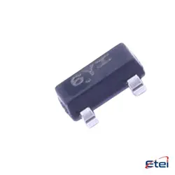
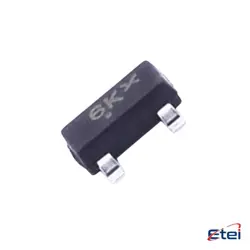
Imagens apenas para referência
MMBFJ175LT1G
+Lista de MateriaisJFET P-CH 30V 0.225W SOT23-3
-
Fabricanteonsemi
-
Peça do Fabricante #MMBFJ175LT1G
-
Pacote SOT-23-3
-
Em Estoque2714
365 Garantia de Qualidade em 1 dia
7*24 Garantia de serviço em 24 horas
90-Garantia de pós-venda em 1 dia
Garantia de Produto Genuíno
Especificações
| Atributo | Valor |
| Package / Case | Tape & Reel (TR),Cut Tape (CT) |
| Part Status | Active |
| FET Type | P-Channel |
| Voltage - Breakdown(V(BR)GSS) | 30 V |
| Current - Drain(Idss) @ Vds(Vgs=0) | 7 mA @ 15 V |
| Voltage - Cutoff(VG Soff) @ Id | 3 V @ 10 nA |
| Input Capacitance(Ciss)(Max) @ Vds | 11pF @ 10V (VGS) |
| Rds On | 125 Ohms |
| Power - Max | 225 mW |
| Operating Temperature | -55°C ~ 150°C (TJ) |
| Mounting Type | Surface Mount |
Visão Geral
Description
The device typically comes in a small SOT-23 package, which is advantageous for saving space on circuit boards, especially in compact electronic designs. Given its specifications, it is often utilized in consumer electronics, industrial controls, and other applications where space and efficient power handling are critical. The MMBFJ175LT1G is noted for its ability to handle moderate power levels, making it a versatile component for engineers and designers looking to optimize circuit performance while maintaining energy efficiency.
Equivalent
1. J175 (generic)
2. 2N5457 (similar specs)
3. BF245 (different pinout)
4. PN4393 (alternative)
5. NTE457 (NTE Electronics equivalent)
Ensure compatibility by verifying specific parameters such as pinch-off voltage, drain current, and package type before substituting.
Features
1. Package Type: Available in a compact SOT-23 package, making it suitable for space-constrained designs.
2. P-Channel: This device is a P-channel JFET, which means it controls current between the source and drain terminals under the influence of a negative gate-source voltage.
3. Low Noise: It offers low noise operation, which is beneficial in audio and RF applications where signal integrity is crucial.
4. High Input Impedance: JFETs inherently have high input impedance, reducing the load on preceding circuit stages.
5. Low On-State Resistance: Allows efficient switching with minimal power loss.
6. Voltage Rating: Typically operates with a drain-source voltage up to -25V, suitable for various low-voltage applications.
7. RoHS Compliant: It is lead-free and complies with Restriction of Hazardous Substances (RoHS) directives, suitable for environmentally-conscious manufacturing processes.
These features make the MMBFJ175LT1G a versatile choice for designers needing reliable performance in low-power switching and amplification tasks.
Pinout
1. Gate (G): This pin is used to control the conductivity between the source and drain. By applying a voltage to the gate, you can modulate the current flow through the device.
2. Source (S): This is the source of charge carriers. For a P-channel JFET, the source is where holes (positive charge carriers) enter the device.
3. Drain (D): This is where the charge carriers exit the device.
The MMBFJ175LT1G is used in various applications, including switching and amplifier circuits, due to its ability to handle low-level signals with low noise.