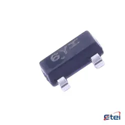
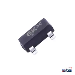
Imagens apenas para referência
MMBFJ177
+Lista de MateriaisJFET P-CH 30V 0.225W SOT23
-
Fabricanteonsemi
-
Peça do Fabricante #MMBFJ177
-
Pacote SOT-23-3
-
Em Estoque4476
365 Garantia de Qualidade em 1 dia
7*24 Garantia de serviço em 24 horas
90-Garantia de pós-venda em 1 dia
Garantia de Produto Genuíno
Especificações
| Atributo | Valor |
| Package / Case | Tape & Reel (TR),Cut Tape (CT) |
| Part Status | Obsolete |
| FET Type | P-Channel |
| Voltage - Breakdown(V(BR)GSS) | 30 V |
| Current - Drain(Idss) @ Vds(Vgs=0) | 1.5 mA @ 15 V |
| Voltage - Cutoff(VG Soff) @ Id | 800 mV @ 10 nA |
| Rds On | 300 Ohms |
| Power - Max | 225 mW |
| Operating Temperature | -55°C ~ 150°C (TJ) |
| Mounting Type | Surface Mount |
Visão Geral
Description
To understand MMBFJ177 better, you would typically need to consider the context in which it is used. For example, if it is an electronic component, you would look at its specifications, such as voltage, current ratings, and intended application. If it’s a newer product or a less common part, detailed information might be available through industry-specific resources, company catalogs, or directly from the manufacturer.
If you have access to the datasheets or technical documents, they can provide precise information, including its features, applications, and compatible systems. For the most accurate and detailed understanding, consulting resources like engineering forums, industry contacts, or direct inquiry with the manufacturer would be advisable.
Equivalent
Features
1. Type: N-channel JFET.
2. Drain-Source Voltage (V_DS): Typically around 25V.
3. Gate-Source Voltage (V_GS): Usually rated at -25V.
4. Drain Current (I_D): It can handle around 10mA to 20mA.
5. Gate-Source Cutoff Voltage (V_GS(off)): Generally between -0.5V to -5V.
6. Low Noise: Designed for low-noise amplification.
7. High Gain: Offers good voltage gain, making it suitable for amplification purposes.
8. Package Type: Often available in SOT-23 or similar surface-mount packages.
9. Applications: Commonly used in audio applications, RF amplifiers, and other analog circuits requiring a low-noise, high-gain component.
10. Temperature Range: Typically operates within a range suitable for most electronic applications, like -55°C to +135°C.
These features make the MMBFJ177 suitable for precision and low-noise amplification applications.
Pinout
1. Source (S): This is the terminal where the current enters the JFET. It is often connected to the more negative side of the power supply for P-channel devices.
2. Gate (G): This is the control terminal. By applying a voltage to the gate, you can control the flow of current between the source and drain.
3. Drain (D): This is the terminal where the current exits the JFET. For the MMBFJ177, current flows from source to drain when the device is on.
These transistors are used due to their high input impedance and low noise characteristics, making them suitable for RF amplification and signal processing applications.
Manufacturer
Application
1. Signal Amplification: Used in low-power amplification circuits, such as audio and RF amplifiers.
2. Switching Circuits: Ideal for fast switching in digital circuits due to its quick response time.
3. Voltage Regulation: Employed in voltage regulation and stabilization circuits.
4. Oscillators: Serves in oscillator circuits for generating repetitive signals.
5. Signal Processing: Utilized in processing analog signals in communication devices.
These features make MMBFJ177 suitable for consumer electronics, telecommunications, and computing devices where efficiency and speed are crucial.