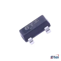
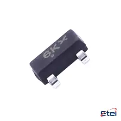
Imagens apenas para referência
MMBFJ201
+Lista de MateriaisJFET N-CH 40V 350MW SOT23
-
Fabricanteonsemi
-
Peça do Fabricante #MMBFJ201
-
Pacote SOT-23
-
Em Estoque5102
365 Garantia de Qualidade em 1 dia
7*24 Garantia de serviço em 24 horas
90-Garantia de pós-venda em 1 dia
Garantia de Produto Genuíno
Especificações
| Atributo | Valor |
| Package / Case | Tape & Reel (TR),Cut Tape (CT) |
| Part Status | Active |
| FET Type | N-Channel |
| Voltage - Breakdown(V(BR)GSS) | 40 V |
| Current - Drain(Idss) @ Vds(Vgs=0) | 200 µA @ 20 V |
| Voltage - Cutoff(VG Soff) @ Id | 300 mV @ 10 nA |
| Power - Max | 350 mW |
| Operating Temperature | -55°C ~ 150°C (TJ) |
| Mounting Type | Surface Mount |
Visão Geral
Description
To provide a general overview, an introductory course labeled as "MMBFJ201" could cover fundamental concepts and principles in its respective field. Such a course might outline core theories, methodologies, and applications necessary for advanced study. It often includes lectures, readings, and discussions, designed to equip students with a foundational understanding of the subject.
Students in this course might explore both theoretical frameworks and practical examples to understand the significance and real-world applications of the material. Additionally, assessments could include assignments, projects, or exams to evaluate comprehension and analytical abilities.
For precise details, refer to the course syllabus or consult the academic institution offering MMBFJ201. They would provide specific information regarding the topics covered, learning outcomes, prerequisites, and any required materials.
Equivalent
Features
1. Type: N-channel JFET.
2. Package: Typically available in a small SOT-23 package, suitable for surface mount applications.
3. Drain-Source Voltage (V_DS): Maximum of 25V.
4. Gate-Source Voltage (V_GS): Typically around ±20V.
5. Drain Current (I_D): Maximum continuous current is around 50mA.
6. Gate-Source Cutoff Voltage (V_GS(off)): Typically ranges from -0.3V to -3.0V.
7. Forward Transfer Admittance (Yfs): Approximately 4.5 mS, indicating the gain of the device.
8. Low Noise: Designed for low-noise amplification, making it suitable for audio applications and high-frequency circuits.
9. High Input Impedance: Ensures minimal loading on preceding stages.
10. Applications: Commonly used in amplifiers, switching circuits, and signal processing tasks.
11. Operating Temperature Range: Typically from -55°C to +150°C.
These features make the MMBFJ201 suitable for various analog and RF applications requiring high performance and reliability.
Pinout
1. Gate (G): This is the control terminal that modulates the conductivity between the source and drain. By applying a voltage to the gate, you control the flow of current through the device.
2. Source (S): This is the terminal through which carriers enter the channel. For an N-channel JFET like the MMBFJ201, this would typically be connected to a lower voltage side in the circuit.
3. Drain (D): This is the terminal through which carriers exit the channel. It is typically connected to a higher voltage side.
The MMBFJ201 is utilized in applications requiring low noise and high input impedance, such as amplifiers and switching applications.
Manufacturer
Application
1. Audio Amplifiers: It is utilized in the input stage of audio circuits for its low noise characteristics.
2. RF Amplifiers: Suitable for high-frequency applications due to its low capacitance.
3. Switching Circuits: Used for fast switching operations.
4. Sensor Interfaces: Ideal for interfacing with sensors due to its high input impedance.
5. Analog Signal Processing: Employed in analog circuits for amplification and buffering.
These features make the MMBFJ201 suitable for various precision and low-noise applications.